The project involves designing and implementing a custom processor in an FPGA using the Verilog hardware description language. The goal of the project was to create a simple processor capable of executing basic instructions such as MOV, JMP, ADD, and other arithmetic and logical operations, with the ability to handle conditional jumps. The processor was implemented in a modular manner, including registers, a control unit, an ALU, program and data memory, as well as a program counter (PC). This implementation allows for understanding and testing the fundamentals of CPU architecture while maintaining flexibility in modifying existing instructions and developing new solutions such as interrupts and pipelining.
The project focuses on designing and implementing a custom, simplified processor architecture in an FPGA (using Verilog), featuring a basic instruction set (including MOV, ADD, JMP) along with external program and data memory. This enables the execution of small instruction sequences and the observation of typical CPU components, such as program counters (PC), general-purpose registers, and the arithmetic-logic unit (ALU).
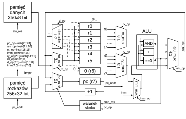
1. Program and Data Memory
- Instruction Memory has an organization of 256×32 bits, meaning it can store a maximum of 256 instructions, each occupying 32 bits. The address signal of this memory (
pc_addr) comes from the program counter register (pc), and the memory output (instr) is then decoded. - Data Memory (256×8 bits) is used to store temporary values, variables, and other necessary data during program execution. The address of this memory usually comes from the ALU output (
alu_res), and data can be written to or read from it depending on the type of instruction.
2. Registers and Instruction Decoder
- General-purpose registers:
r0–r5, which can store data and operation results. - Register
r6is set to the value 0 in this project (which facilitates comparison with zero or data initialization). - Register
r7functions as the Program Counter (PC). Its output is used by instruction memory to fetch the next instruction. - Decoder breaks the 32-bit instruction into individual fields (e.g.,
pc_op,alu_op,rx_op,ry_op,rd_op,imm_op, and an optional 8-bit immediate fieldimm[7:0]).
These signals allow different CPU blocks (ALU, multiplexers, registers) to „know” how to respond to a specific instruction.
3. ALU (Arithmetic Logic Unit)
The ALU (Arithmetic Logic Unit) takes two operands:
- Operand X – selected by the multiplexer
rx_mux, contains the value from one of the registersr0–r15or the value 0 fromr6. - Operand Y – selected by the multiplexer
ry_mux(e.g., another register value or the immediate valueimm).
Depending on the instruction (alu_op), the ALU can:
- Perform addition (
+). - Perform logical operations (e.g., AND).
- Check equality with zero (
==0) – which facilitates the implementation of comparison instructions and conditional jumps.
The result from the ALU (alu_res) can be stored in the destination register (e.g., via rd_op), used as a data memory address, or as a new PC address in the case of a jump.
4. Jump Control and PC Update
- PC (
r7) is incremented by 1 after each executed instruction, meaning instructions are executed sequentially. - If an instruction requires a jump (e.g., based on the
CMPoperation), a new value may be loaded into the PC register – for example, from the ALU output or an immediate field of the instruction. - The „jump condition” block (
cmp_res) determines whether the PC is assigned a new address or continues counting sequentially.
5. Example Instruction Execution Flow
- Instruction Fetch: PC (
r7) points to the address in the instruction memory (256×32). A 32-bit word is fetched into the decoder. - Decoding: The decoder extracts fields defining the instruction type, target registers, and any immediate values.
- Operand Preparation: The multiplexers
rx_muxandry_muxselect the correct data sources (e.g., registersr0–r5,r6=0, or the immediate valueimm). - ALU Operation: Based on
alu_op, the ALU performs addition, AND, or comparison. - Result Storage: The ALU result can be written to a destination register, stored in memory, or used as a jump address.
- PC Update: If the instruction is a jump and the condition is met, PC takes the value from the ALU; otherwise, PC is incremented (
PC+1).
6. Applications and Development
The designed processor can execute basic instructions such as MOV, ADD, AND, CMP, JMP, JE, HLT, etc. It is suitable for learning CPU architecture and FPGA implementation. Possible further developments include adding additional instructions, implementing interrupts or pipelining, as well as expanding memory and cache layers.
Thanks to its simple, modular design and clear separation of instruction and data memory, the project is easy to modify and can serve as a starting point for advanced experiments with custom microarchitectures in programmable circuits.